Quick Start
In this section we will walk through the process of compiling, simulating, and running a ReWire program. The purpose of this tutorial is not to help you understand the ReWire language, just how to use the ReWire compiler.
We will be working with every functional programmer’s favorite example: the Fibonacci sequence. The Fibonacci sequence is defined as 0, 1, 1, 2, 3, 5, 8, 13, … . In other words, the first two elements of the sequence are 0 and 1, and the nth element of the sequence (for n > 1) is obtained by adding together the two elements that precede it. We will use ReWire to build a circuit that displays one element of the Fibonacci sequence per clock tick, in order, in 8-bit binary on a bank of LEDs.
The following block diagram illustrates the inputs and outputs of the circuit. The one-bit pause input will cause the circuit to pause operation (i.e., hold its current value) when high; it will be connected to a toggle switch. The outputs fib[0:7] are to be connected to the LEDs on the FPGA board.
     ______________________
     |                    |
  ---| pause              |
     |           fib[0:7] |-/-
  ---|>                   |
     |____________________|
This tutorial was written with a Spartan-3E Starter Kit board in mind, though it should not be hard to adapt the example to different Xilinx boards. Since the Spartan-3E Starter Kit has been discontinued, we will soon be updating this example to run on a newer board.
Source Code
The source code for our example comes in two pieces: Fibonacci.hs, which is a Haskell source file, and prims.vhd, which contains the code for a natively defined VHDL function plusW8. These files are available in the ReWire source tree at /examples/Fibonacci. For purposes of this tutorial, you don’t need to worry about the exact meaning of this code, but one point is important to note up front. Every ReWire program must have a symbol named start whose type is of the form ReT i o I (), where i and o are the type of the circuit’s input and output respectively. (The clock input is always implicitly present.)
In this case, our circuit takes a one-bit input and produces an eight-bit word as output, so we have (in Fibonacci.hs):
start :: ReT Bit W8 I ()
start = begin
The example source code in its entirety follows.
Fibonacci.hs
--
-- The compiler doesn't yet support a "prelude" so we will have to define a
-- few things ourselves!
--
data Bit        = Zero | One
data W8         = W8 Bit Bit Bit Bit Bit Bit Bit Bit

plusW8 :: W8 -> W8 -> W8
{-# INLINE plusW8 #-}
plusW8 = nativeVhdl "plusW8" plusW8

zeroW8 :: W8
zeroW8 = W8 Zero Zero Zero Zero Zero Zero Zero Zero

oneW8 :: W8
oneW8 = W8 Zero Zero Zero Zero Zero Zero Zero One

--
-- End stuff that will eventually be in the prelude.
--

start :: ReT Bit W8 I ()
start = begin

begin :: ReT Bit W8 I ()
begin = loop zeroW8 oneW8

loop :: W8 -> W8 -> ReT Bit W8 I ()
loop n m = do b <- signal n
              case b of
                  One  -> loop n m
                  Zero -> loop m (plusW8 n m)
prims.vhd
library ieee;
use ieee.std_logic_1164.all;
use ieee.numeric_std.all;

package prims is
  pure function plusW8 (x : std_logic_vector; y : std_logic_vector) return std_logic_vector;
end prims;

package body prims is
  pure function plusW8 (x : std_logic_vector; y : std_logic_vector) return std_logic_vector is
  begin
	return (std_logic_vector(unsigned(x)+unsigned(y)));
  end plusW8;
end prims;
Building a Circuit from the Example
Getting our ReWire program to run on an FPGA requires two basic steps. First, we use the rwc compiler to translate the Haskell part of the program (here Fibonacci.hs) into VHDL:
     _____________                ______________
    |             \              |              \
    | Fibonacci.hs | --> rwc --> | Fibonacci.vhd |
    |______________|             |_______________|
Second, we hand off the resulting VHDL file, along with our prims.vhd in case our program contains any user-defined native VHDL functions, to a standard VHDL synthesis toolchain like ISE or Vivado:
     ______________
    |              \
    | Fibonacci.vhd |---.
    |_______________|   |
                        +---> VHDL toolchain (ISE, Vivado, ...)
     ______________     |
    |              \    |
    |   prims.vhd   |---'
    |_______________|
Step 1: Running rwc
The first step, running the compiler, is straightforward. The command:
$ rwc [sourcefile.hs] -o [destfile.vhd]
will compile the file sourcefile.hs and generate VHDL that will be saved in the file destfile.vhd. So for our example we invoke the compiler as follows:
$ cd ReWire/examples/Fibonacci        # or wherever you have placed the source files listed above
$ rwc Fibonacci.hs -o Fibonacci.vhd
This will generate a VHDL file called Fibonacci.vhd which is ready for simulation and synthesis. The top-level entity in this VHDL file is called rewire and has the following declaration:
entity rewire is
  Port ( clk : in std_logic ;
         input : in std_logic_vector (0 to 0);
         output : out std_logic_vector (0 to 7));
end rewire;
In fact, the ReWire compiler will always produce a VHDL entity named rewire with ports named clk, input, and output. The width of input and output (here 1 and 8 bits respectively) are determined by the type of start.
Step 2: Creating an ISE Project
Having generated VHDL for our Fibonacci circuit, the next step is to import that VHDL into the ISE Design Suite. First, open the ISE Project Navigator. (FIXME double-check this: On Windows, this is likely found in Start -> Xilinx -> ISE Design Suite -> Project Navigator. If you are using Linux, please refer to the ISE documentation.)
You should be greeted first with a splash screen, then with the main Project Navigator window, which looks something like this:
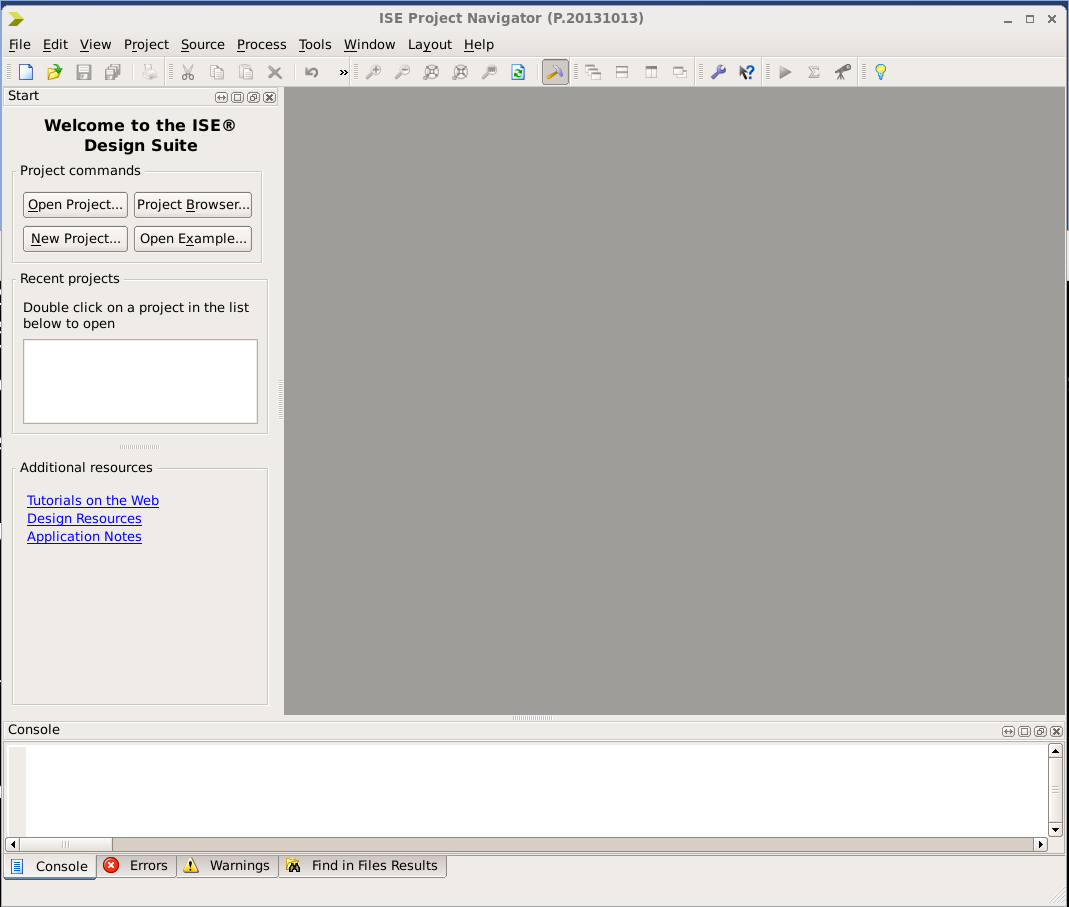
You wil need to create a new ISE project. Select File -> New Project to open the New Project Wizard:
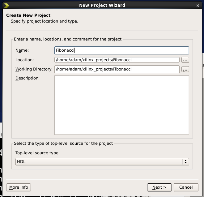
In the box marked Name, enter Fibonacci. In the box marked Location, select a directory in which to store the project. A subdirectory for the new project will automatically be filled in under Working Directory. You do not need to change this. Now, click Next to proceed to the Project Settings screen:
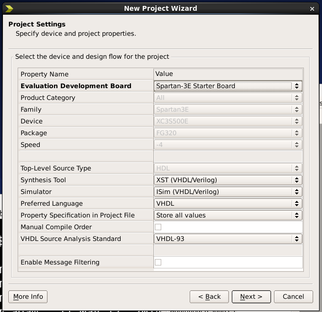
Under Evaluation Development Board, select Spartan-3E Starter Board. Under Preferred Language, select VHDL. Click Next, then click Finish.
You should now have an empty ISE project open in the main Project Navigator window. Now select Project -> Add Copy of Source.
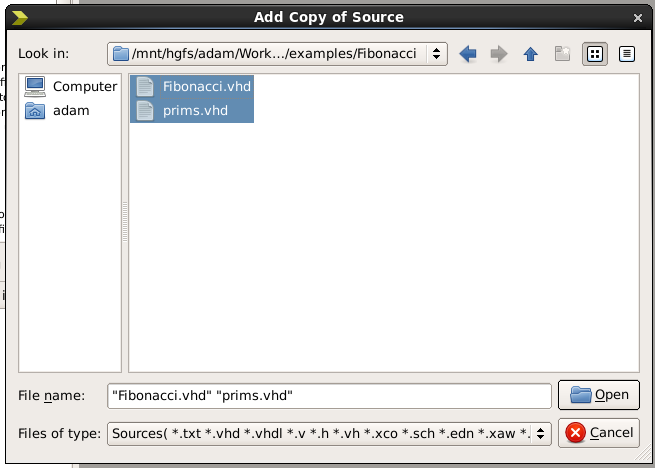
Browse to the directory where the example source files are contained, and select both Fibonacci.vhd and prims.vhd. Then click Open, and click OK on the dialog box that follows.
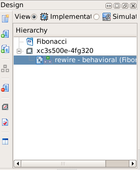
The Fibonacci source files should now show up under the “Design” pane on the left side of the Project Navigator window, with rewire marked as the top-level entity:
Step 3: Simulating the Circuit
Before loading our circuit onto the board, it is advisable to test the circuit in a VHDL simulator and verify correct operation at the behavioral level. ISE comes with a simulator called ISim that we can use for this purpose.
Under the “Design” pane, select Simulation, click on rewire, then open up the submenu labeled “ISim Simulator”:
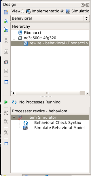
Now double-click Simulate Behavioral Model. The ISim simulator should load. The default settings are a bit over-eager, and will run the simulation for a few microseconds at start up, which (since we haven’t yet provided a defined input) will result in some strange results. To undo this, select Simulation -> Restart. You should now see a window that looks like the following (your display may be showing more signals, but it is just clk, input, and outputs that we are interested in):
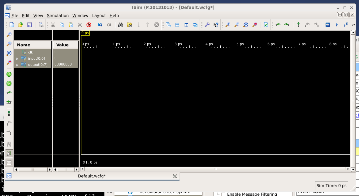
Because our design is a clocked, sequential circuit, we must supply a clock signal. Right click on clk and select Force Clock:
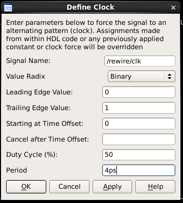
Under Leading Edge Value, enter 0. Under Trailing Edge Value, enter 1. Since we are only simulating at a behavioral level, it does not matter what clock period we choose, since we are assuming that things like gate delay are nil. Just enter 4ps (i.e., 4 picoseconds) under Period. Leave other values at defaults. Click OK.
We must also supply a value for the input. Right click on input and select Force Constant:
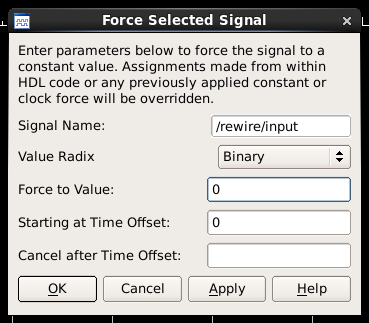
Initially, let’s force the input (i.e. the pause signal) to zero. Enter 0 under Force to Value and click OK.
Now, enter 1ps in the run time field at the upper right corner of the window:

Finally, click the “run for specified time” button (which has a small “play button” symbol and a picture of an hourglass) a few times, and observe the output in the waveform display pane:
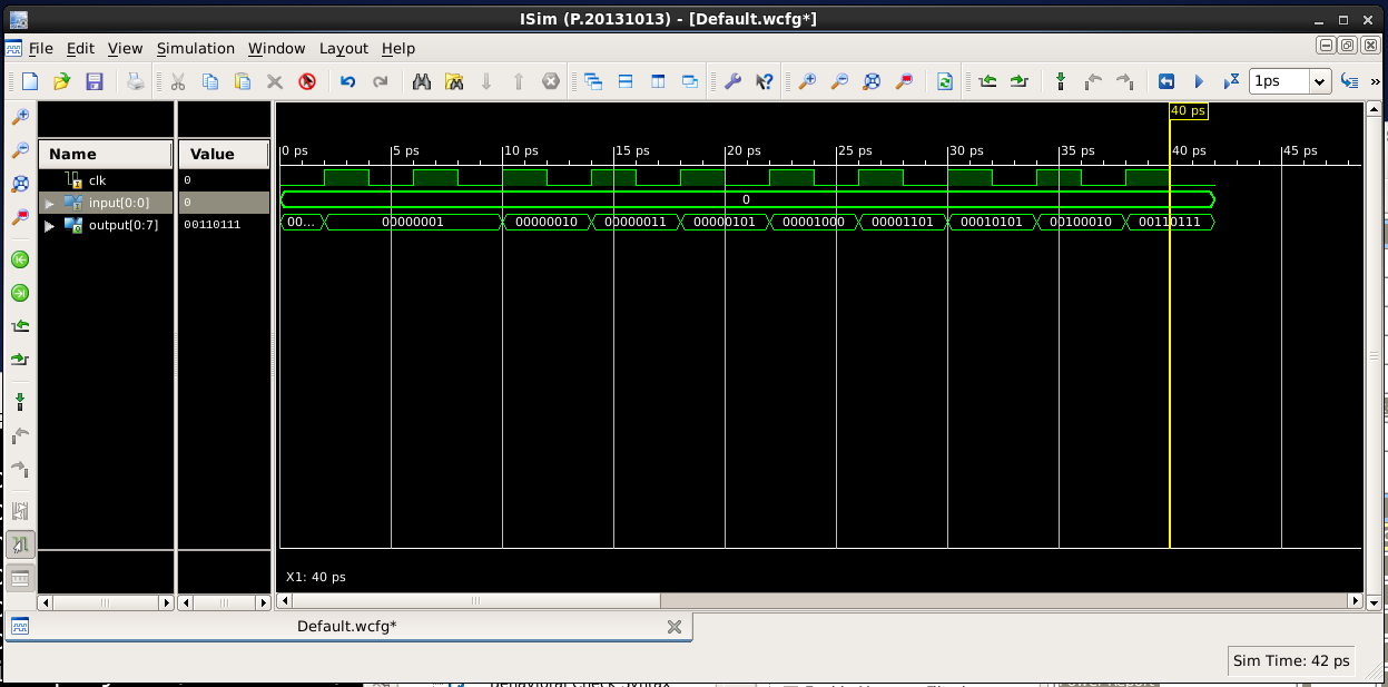
Obviously something is happening, but is it the Fibonacci sequence? To make the output easier to read, right click on output, select Radix, and select Unsigned Decimal. This will change the display value for the output waveform from binary to decimal:
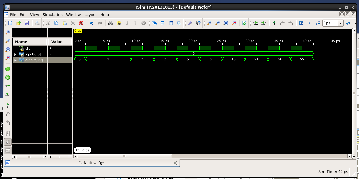
Observe that over the first few clock ticks, the circuit is outputting 0, 1 (for two clock cycles!), 2, 3, 5, 8, 13, 21, 34, 55… these are indeed the first few elements of the Fibonacci sequence!
Finally, we should test to make sure that the pause switch works. Right click on input, select Force Constant, change the value to 1, click OK, then press the “run for specified time” button a few more times:
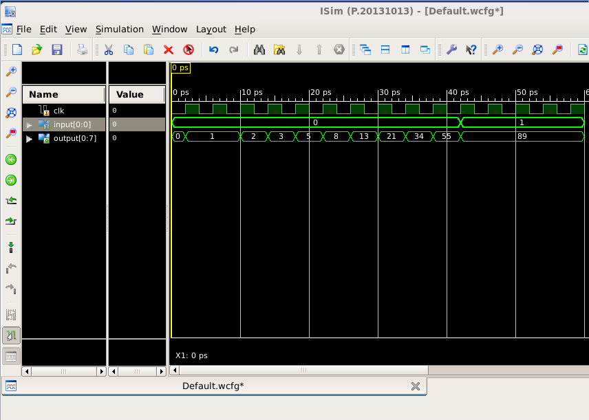
Notice that the value remains unchanged even as the clock continues to tick. Now force the switch back to “off”: right click on input, select Force Constant, change the value to 0, click OK, then press the “run for specified time” button a few more times:
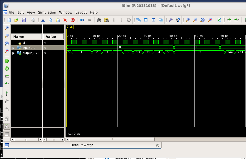
Observe that the circuit resumes operation on subsequent clock ticks. Thus everything seems to be in order! (Note that if the circuit is allowed to run long enough (i.e. past the 13th element of the sequence), the output value will overflow and wrap around. This is the expected behavior; it is, after all, only an example.)
You can now close the ISim window; if you receive a prompt about saving the waveform configuration, you can say no.
Step 4: Implementing the Circuit on the Board
No FPGA project can be considered successful until we have actually made some LEDs flash, so in this section we will load our circuit onto our Spartan-3E Starter Kit board. For testing purposes, we will connect the clock signal to the on-board 50MHz oscillator at FPGA pin C9; the pause input to the switch SW0 at FPGA pin L13; and the output bits to the LEDs located at the lower right corner of the board, at FPGA pins F9, E9, D11, C11, F11, E11, E12, and F12 (from left to right):
                             ______________________
                             |                    |
        switch SW0 [L13] ----| pause              |
                             |           fib[0:7] |-/--- LEDs LD7 through LD0
on-board oscillator [C9] ----|>                   |      [F9,E9,D11,C11,F11,E11,E12,F12]
                             |____________________|
(Obviously our choice of a 50MHz clock will make it impossible to view the sequence in real time, but the pause switch will make it possible to peek in on the sequence.)
To map VHDL inputs and outputs to FPGA pins, we must add a UCF constraint file to our project. First, select Implementation in the Design pane at the upper left corner of the Project Navigator window. Then select Project -> New Source -> Implementation Constraints File. Under File name, enter Fibonacci.ucf, then click Next and click Finish. An editor window for the (new, blank) UCF file will appear. Enter the following text and select File -> Save:
NET "clk" LOC="C9";
NET "input[0]" LOC="L13";
NET "output[0]" LOC="F9";
NET "output[1]" LOC="E9";
NET "output[2]" LOC="D11";
NET "output[3]" LOC="C11";
NET "output[4]" LOC="F11";
NET "output[5]" LOC="E11";
NET "output[6]" LOC="E12";
NET "output[7]" LOC="F12";
With the UCF file added to the project, we can now synthesize and implement our circuit. Select rewire in the Design pane, then under the Processes pane, double-click Implement Design:
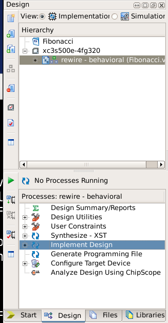
ISE will automatically run the “Synthesize - XST” process, then the “Implement Design” process. If everything goes as expected, you will see a few VHDL-related warnings fly by in the console during the synthesis phase; these may be ignored.
Once the implementation process has finished, double-click Generate Programming File under the Processes pane to generate the bitstream file for configuring the FPGA. Then double-click Configure Target Device. If you are prompted to add an iMPACT project file, click OK.
(FIXME: need to grab some screenshots and flesh out the rest of the process…)